Tang Primer board
2020-06-09
The Tang Primer at a Glance

Tang Primer uses Anlogic's EG4S20 as the core unit, 20K logic unit (LUT4/LUT5 hybrid architecture), approximately 130KB SRAM, built-in 32bit bit width 64MBit SDRAM, rich LVDS pin, built-in 12-bit 1MSPS ADC This provides unlimited possibilities for Tang Primer:
Tang Primer features
- FPC40P socket, can be connected to RGB LCD, VGA adapter board, high speed DAC module.
- FPC24P socket, can be connected to DVP camera, high speed ADC module.
- Resistive touch screen controller for I2C interface, used with RGB LCD.
- 3-channel DCDC power supply chip, stable and efficient power supply, independent adjustment of Bank0 IO level.
- FPGA configuration Flash, 8Mbit User Flash, nor/nand optional.
- Onboard FPGA JTAG Download Debugger.
- Onboard RGB LED
- The adjacent pins LVDS are drawn in the same length, and 8 GCLKs are taken out, and 8 ADCs are all taken out.
- The double row pin spacing is 900 mils and is compatible with breadboard development.
- The half hole leads to an additional 40 IO and the entire board leads to 130+ IO.
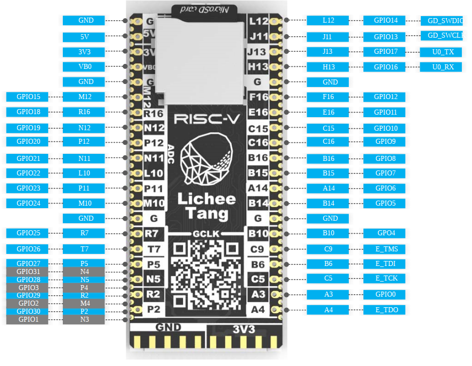
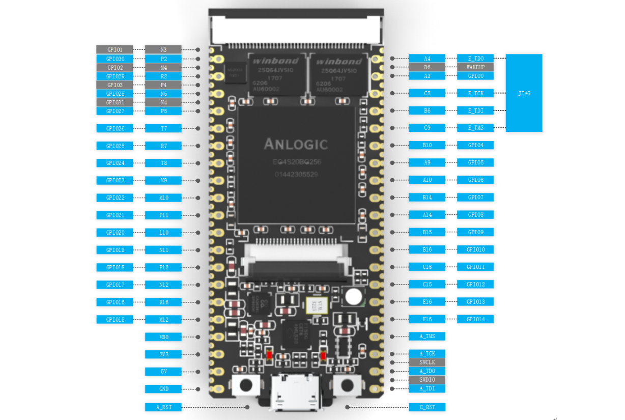
Pinouts
Pinout for New Tang Primer Board.

Pinout for Old Tang Primer Board.


 English
 Translate